CAD design prepare for PCB fabrication assembly
The process of preparing a PCB (Printed Circuit Board) design for fabrication assembly starts with creating a detailed Computer-Aided Design (CAD) model. This model serves as the blueprint for the entire PCB manufacturing process, guiding every step from material selection to component placement. CAD design is a critical first step in ensuring that the final PCB functions as intended and meets all necessary requirements for assembly. The preparation of a CAD design for PCB fabrication assembly involves several key stages, each of which plays a significant role in producing high-quality, reliable PCBs.
The first step in preparing a CAD design for PCB fabrication assembly is to create the initial schematic diagram. A schematic represents the electronic circuit’s layout, showing the interconnections between components such as resistors, capacitors, diodes, and integrated circuits. This step is crucial because it defines the electrical functionality of the PCB. Engineers use the schematic to ensure that all components are correctly connected and that the circuit design is electrically sound before proceeding with the physical layout.
Once the schematic is complete, the next step is to transition from the schematic to a PCB layout. This involves placing the components onto the board, arranging them in a way that optimizes space, signal integrity, and manufacturability. The layout must take into account factors such as the size and shape of the components, trace routing, and the electrical performance of the board. During this phase, engineers use the CAD software to create the physical representation of the PCB, ensuring that each component is placed in a way that will allow for efficient signal flow and minimize interference or other potential electrical issues.
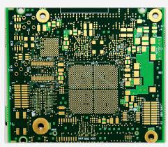
How does a CAD design prepare for PCB fabrication assembly?
After the PCB layout is designed, the CAD software generates a set of files known as Gerber files. These files are the standard format used in the PCB fabrication industry to communicate the design specifications to the manufacturer. Gerber files contain all the necessary information for each layer of the PCB, including the copper traces, pads, vias, and solder mask. These files also include drill files, which specify the locations and sizes of holes to be drilled in the PCB, such as those needed for component leads or vias. The Gerber files serve as a digital map of the PCB that the fabrication assembly team will follow to create the physical board.
Before the CAD design is finalized for pcb fabrication assembly, engineers perform Design for Manufacturability (DFM) checks. DFM is a process that ensures the design is optimized for production and can be fabricated using available manufacturing capabilities. During this phase, the CAD design is checked for potential issues such as traces that are too narrow, components that are too close together, or designs that are difficult to manufacture with current equipment. DFM checks help identify any changes or adjustments that need to be made to ensure the PCB is both functional and feasible to produce.
Another important step in preparing a CAD design for PCB fabrication assembly is the creation of a Bill of Materials (BOM). The BOM is a comprehensive list of all the components required for the PCB, including their part numbers, quantities, and specifications. The BOM is essential for the assembly process, as it ensures that all the necessary parts are available and correctly matched to the PCB design. Inaccuracies or omissions in the BOM can lead to delays in production and assembly, so it is vital that the list is thorough and accurate.
Once the design and supporting documentation are complete, the CAD design is sent to the PCB manufacturer for fabrication. The manufacturer will use the Gerber files, BOM, and other specifications to create the physical PCB. During this process, various fabrication steps are performed, including etching the copper traces, applying the solder mask, and adding the silkscreen layer. The design files guide each of these processes, ensuring that the final PCB matches the specifications laid out in the CAD design.
After fabrication, the PCB is ready for assembly, where components are placed on the board, soldered, and tested. The accuracy and precision of the original CAD design are critical during the PCB fabrication assembly phase to ensure that the components are correctly placed and connected, and the board functions as intended.
In conclusion, the preparation of a CAD design for PCB fabrication assembly is a detailed and multi-step process. It involves creating a schematic, designing the PCB layout, generating Gerber files, performing DFM checks, and compiling a BOM. These steps ensure that the design is both electrically functional and manufacturable. A well-prepared CAD design sets the foundation for a smooth and efficient PCB fabrication assembly process, ultimately leading to the creation of high-quality, reliable PCBs for use in a wide range of electronic devices.